Next-generation Chiplet and Advanced Packaging Architectures
Scaling Semiconductor Innovation Through Modular Architectures
AI and high-performance computing (HPC) workloads are increasing requirements for compute density, memory bandwidth, power efficiency, and scalability, challenging conventional monolithic processor designs.
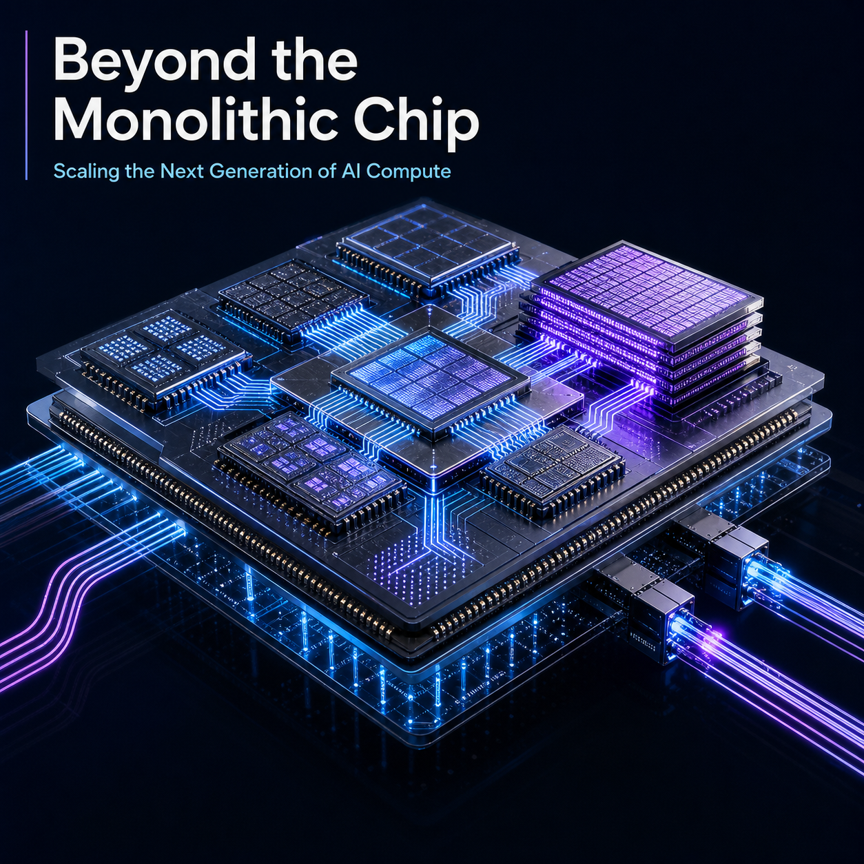
Chiplet architectures, HBM, and advanced packaging are creating new pathways to system-level performance through modular design, heterogeneous integration, and tighter compute-memory connectivity. Frost & Sullivan’s analysis examines the technologies, ecosystem developments, and growth opportunities shaping this transition.
Next-Generation Chiplet and Advanced Packaging Architectures: Redefining Performance and Scalability in AI and HPC
Explore Next-generation Chiplet Architectures

What the Analysis Covers
Next-generation chiplet architectures and advanced packaging technologies
UCIe and the evolution of interoperable, multi-vendor chiplet platforms
HBM3E and HBM4 integration for memory-intensive AI workloads
2.5D/3D packaging, hybrid bonding, and heterogeneous integration
Emerging optical chiplets and co-packaged optics
Leading AI and HPC chiplet implementations
Growth opportunities across chiplets and advanced packaging
Where the Next Growth Opportunities Are Emerging
UCIe-based Multi-vendor Chiplet Platforms
Open die-to-die standards are creating opportunities for interoperable architectures spanning compute, memory, and input/output (I/O).
Opportunity Size: Over USD 1 billion in 5 years
Timeline for Action: 3–5 years
HBM4-ready 2.5D/3D Packaging Platforms
Next-generation AI accelerators are creating demand for advanced packaging capable of supporting higher memory bandwidth, compute density, and thermal requirements.
Opportunity Size: Over USD 1 billion in 5 years
Timeline for Action: 3–5 years
Decisions Semiconductor Leaders Must Make Now
- Where should investments be prioritized across chiplets, HBM, packaging, and interconnect technologies?
- How can UCIe support more interoperable and scalable architectures?
- Which advanced packaging capabilities will be critical for next-generation AI and HPC?
- What ecosystem partnerships are needed to accelerate commercialization?
Who Will Benefit from This Analysis?
Semiconductor executives, R&D and technology leaders, product strategists, foundries, integrated device manufacturers (IDMs), fabless semiconductor companies, outsourced semiconductor assembly and test (OSAT) providers, electronic design automation (EDA) providers, hyperscalers, and investors evaluating the future of AI and HPC semiconductor architectures.
Sign up for a complimentary Growth Pipeline Dialog™
A Growth Pipeline Dialog is a structured discussion with our growth experts providing unparalleled technology intelligence and proven implementation best practices. This discussion will spark innovative thinking and help generate a pipeline of growth opportunities you can leverage to maximize your company’s future growth potential.
Upon completing the dialog session, you will receive a $1,000 honorarium as a token of our appreciation, which can be used towards the purchase of our products or services.